PMC51x LoRa Module Specification
PMC51x is a Mini-PCIe LoRa module used as the LoRa radio component of the GD6 series LoRaWAN gateways. This document describes its functions, technical specifications, pin definitions, interface requirements, and model selection.
1. Product Overview
1.1 Positioning and GD6 Relationship
PMC51x is the LoRa radio component of GD6 and connects to the host through a Mini-PCIe form factor. It is based on the Semtech SX1302 LoRa baseband chip, with a pin-compatible SX1303 option available for project customization. The module operates in half-duplex mode, communicates with the host over SPI, and supports the Semtech open-source Packet Forwarder.
The final digit in PMC514 and PMC518 identifies the radio-frequency family; it does not indicate the number of LoRaWAN channels:
- PMC514: 400 MHz family, including EU433 and CN470.
- PMC518: 800 MHz and higher family, including EU868, AS923, AU915, US915, and KR920.
1.2 Key Features
- Standard Mini-PCIe form factor for straightforward integration and replacement.
- SX1302 baseband with a customizable pin-compatible SX1303 option.
- SPI host interface and PPS timing input.
- EU433, CN470, EU868, AS923, AU915, US915, and KR920 regional standards.
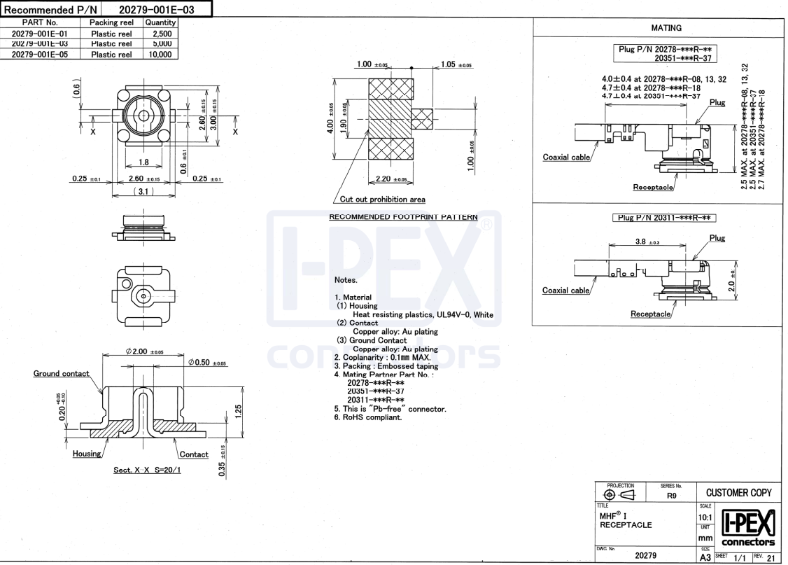
- First-generation I-PEX antenna connector.
- Eight parallel receive paths with SF5–SF12 support.
- Receive sensitivity down to -141 dBm.
- One transmit path with up to 22 dBm output power.
- Built-in power-on reset sequencing to simplify host control.
2. Product Views
2.1 Front View
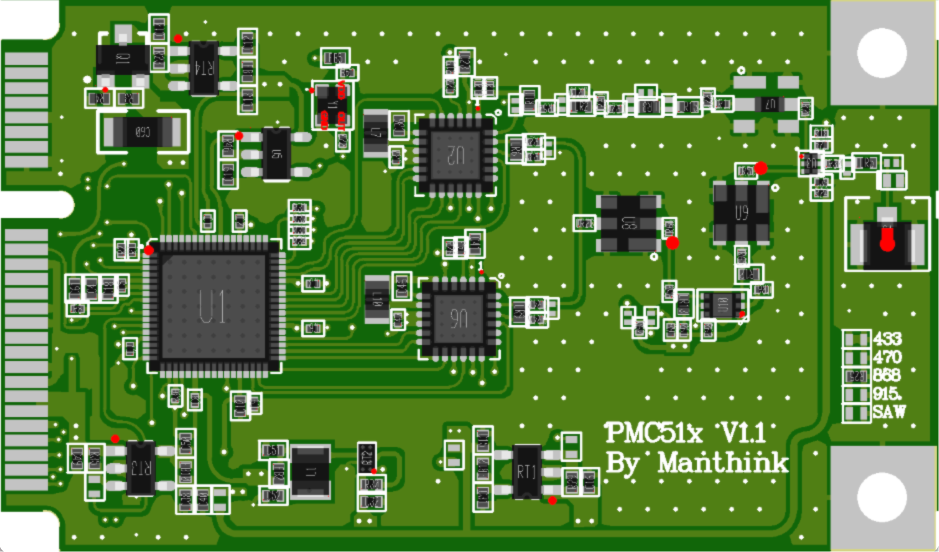
2.2 Bottom View
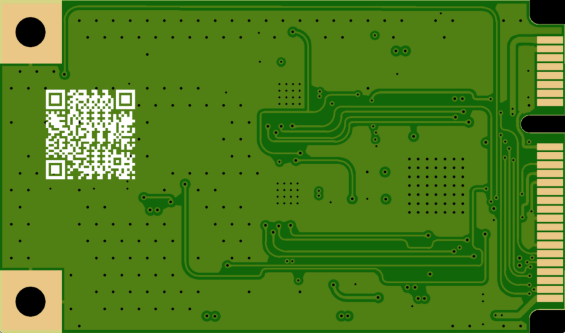
3. Technical Specifications
3.1 Electrical and Mechanical Specifications
| Item | Specification |
|---|---|
| Form factor | Mini-PCIe |
| Dimensions | 30.0 mm × 51.0 mm × 4.5 mm |
| Host interface | SPI |
| Operating mode | Half-duplex |
| Supply voltage | DC 3.3–5 V |
| Transmit current | < 120 mA |
| Receive current | < 60 mA |
| Operating temperature | -40 to +85 °C |
| Antenna connector | First-generation I-PEX |
3.2 Radio Specifications
| Item | Specification |
|---|---|
| Baseband chip | SX1302; customizable pin-compatible SX1303 |
| Receive paths | 8 |
| Transmit paths | 1 |
| Spreading factors | SF5–SF12 |
| Receive sensitivity | Down to -141 dBm |
| Maximum transmit power | 22 dBm |
| EU433 | 433–434 MHz |
| CN470 | 470–510 MHz |
| EU868 | 863–870 MHz |
| AS923 | 920–928 MHz |
| AU915 | 915–928 MHz |
| US915 | 902–928 MHz |
| KR920 | Configured according to KR920 regional parameters |
4. Mini-PCIe Pin Definition
4.1 Signal Types
| Abbreviation | Meaning |
|---|---|
| PI | Power input |
| DI | Digital input |
| DO | Digital output |
| IO | Bidirectional digital signal |
| NC | Not internally connected |
| RESERVED | Reserved signal |
4.2 Main Pins
| Function | Pins | Description |
|---|---|---|
| GND | 4, 9, 15, 18, 21, 26, 27, 29, 34, 35, 37, 40, 43, 50 | Power ground |
| VCC_3V3 | 2, 24, 39, 41, 52 | Power input |
| PPS | 19 | GPS PPS timing input |
| NRESET | 22 | Module reset, active high |
| RX_ON | 42 | Receive-state output connected to the onboard indicator |
| TX_ON | 44 | Transmit-state output connected to the onboard indicator |
| SX_SCK | 45 | SPI clock input |
| CFG_ON | 46 | Configuration-state output connected to the onboard indicator |
| SX_MISO | 47 | SPI data output |
| SX_MOSI | 49 | SPI data input |
| SX_CSN | 51 | SPI chip-select input |
4.3 Complete 52-Pin Definition
| Pin | Mini-PCIe Name | Module Signal | Type | Description |
|---|---|---|---|---|
| 1 | WAKE# | RESERVED | DO | Reserved for pass-through variants; leave floating |
| 2 | 3.3Vaux | VCC_3V3 | PI | Power input |
| 3 | COEX1 | NC | — | Not internally connected; leave floating |
| 4 | GND | GND | — | Power ground |
| 5 | COEX2 | NC | — | Not internally connected; leave floating |
| 6 | 1.5V | NC | — | Not used |
| 7 | CLKREQ# | NC | — | Not internally connected; leave floating |
| 8 | UIM_PWR | NC | — | Not used |
| 9 | GND | GND | — | Power ground |
| 10 | UIM_DATA | RESERVED | IO | Reserved for pass-through variants; leave floating |
| 11 | REFCLK- | RESERVED | DI | Reserved for pass-through variants; leave floating |
| 12 | UIM_CLK | RESERVED | IO | Reserved for pass-through variants; leave floating |
| 13 | REFCLK+ | RESERVED | DO | Reserved for pass-through variants; leave floating |
| 14 | UIM_RESET | NC | — | Not used |
| 15 | GND | GND | — | Power ground |
| 16 | UIM_VPP | NC | — | Not internally connected; leave floating |
| 17 | RESERVED | NC | — | Not internally connected; leave floating |
| 18 | GND | GND | — | Power ground |
| 19 | RESERVED | PPS | DI | GPS PPS timing input; may be left floating when unused |
| 20 | W_DISABLE# | NC | — | Not internally connected; leave floating |
| 21 | GND | GND | — | Power ground |
| 22 | PERST# | NRESET | DI | Reset control, active high |
| 23 | PERn0 | RESERVED | DI | Reserved; leave floating |
| 24 | 3.3Vaux | VCC_3V3 | PI | Power input |
| 25 | PERp0 | NC | — | Not used |
| 26 | GND | GND | — | Power ground |
| 27 | GND | GND | — | Power ground |
| 28 | 1.5V | NC | — | Not used |
| 29 | GND | GND | — | Power ground |
| 30 | SMB_CLK | NC | — | Not internally connected; leave floating |
| 31 | PETn0 | RESERVED | DO | Reserved; leave floating |
| 32 | SMB_DATA | NC | — | Not internally connected; leave floating |
| 33 | PETp0 | NC | — | Not used |
| 34 | GND | GND | — | Power ground |
| 35 | GND | GND | — | Power ground |
| 36 | USB_D- | RESERVED | IO | Reserved for pass-through variants; leave floating |
| 37 | GND | GND | — | Power ground |
| 38 | USB_D+ | RESERVED | IO | Reserved for pass-through variants; leave floating |
| 39 | 3.3Vaux | VCC_3V3 | PI | Power input |
| 40 | GND | GND | — | Power ground |
| 41 | 3.3Vaux | VCC_3V3 | PI | Power input |
| 42 | LED_WWAN# | RX_ON | DO | Receive-state indicator connected to the onboard LED |
| 43 | GND | GND | — | Power ground |
| 44 | LED_WLAN# | TX_ON | DO | Transmit-state indicator connected to the onboard LED |
| 45 | RESERVED | SX_SCK | DI | SPI clock input |
| 46 | LED_WPAN# | CFG_ON | DO | Configuration-state indicator connected to the onboard LED |
| 47 | RESERVED | SX_MISO | DO | SPI data output |
| 48 | 1.5V | NC | — | Not used |
| 49 | RESERVED | SX_MOSI | DI | SPI data input |
| 50 | GND | GND | — | Power ground |
| 51 | RESERVED | SX_CSN | DI | SPI chip-select input |
| 52 | 3.3Vaux | VCC_3V3 | PI | Power input |
5. Interface Details
5.1 Power Interface
The module is powered through the Mini-PCIe VCC_3V3 pins and operates from DC 3.3–5 V. The host must provide a stable supply with enough headroom for the transmit peak current and should place decoupling capacitors close to the module. All GND pins must be connected reliably.
5.2 SPI Interface
The SPI signals are SX_SCK, SX_MISO, SX_MOSI, and SX_CSN. The host SPI controller must support full-duplex communication. Refer to the Semtech SX1302 data sheet for timing, electrical limits, and register-access procedures.
5.3 Control and Status Interfaces
| Signal | Direction | Function |
|---|---|---|
| PPS | Input | External GPS PPS timing |
| NRESET | Input | Module reset, active high |
| RX_ON | Output | Receive operating state |
| TX_ON | Output | Transmit operating state |
| CFG_ON | Output | Configuration operating state |
6. Signal Behavior
6.1 PPS
The PPS pin accepts a one-pulse-per-second signal from a GPS module so that packets can carry precise timestamps. The pin may be left floating when PPS is not used.
6.2 NRESET
To reset the module, drive NRESET high for 0.05–0.2 s and then release it. Keep the reset trace short and shield it with an adjacent ground trace where practical to reduce the risk of unintended resets.
6.3 RX_ON, TX_ON, and CFG_ON
RX_ON is high while the module is receiving, TX_ON is high while it is transmitting, and CFG_ON indicates the configuration state. These signals are connected to onboard LEDs and are associated with SX1302 GPIOs.
7. Antenna Interface
The module uses a first-generation I-PEX antenna receptacle. Use a matching RF cable and antenna, and ensure that the antenna band matches the module model and deployment region. The RF routing and mechanical design should avoid applying lateral stress to the connector.
8. Models and Regional Standards
| Model | Frequency Family | Supported Regional Standards |
|---|---|---|
| PMC514-433-N | 400 MHz | EU433 |
| PMC514-470-N | 400 MHz | CN470 |
| PMC518-868-N | 800 MHz and higher | EU868 |
| PMC518-915-N | 800 MHz and higher | AS923, AU915, US915, KR920 |
Select a model and regional configuration that comply with local regulations. The "4" or "8" in the model family identifies its frequency range; it does not indicate the number of receive or transmit channels.
9. Integration and Safety Notes
- Disconnect power before installing or removing the module.
- Apply ESD precautions and avoid touching RF components or the edge connector directly.
- Connect the correct antenna before transmission and verify that its band and impedance match the module.
- Do not use NC or RESERVED pins for undocumented functions.
- Ensure the host enclosure keeps the module within its -40 to +85 °C operating range.
- The final product's radio parameters, transmit power, and deployment region must meet applicable regulations and certification requirements.
10. Contact
- Website: www.manthink.cn
- Email: info@manthink.cn
- Phone: +86 15810684257